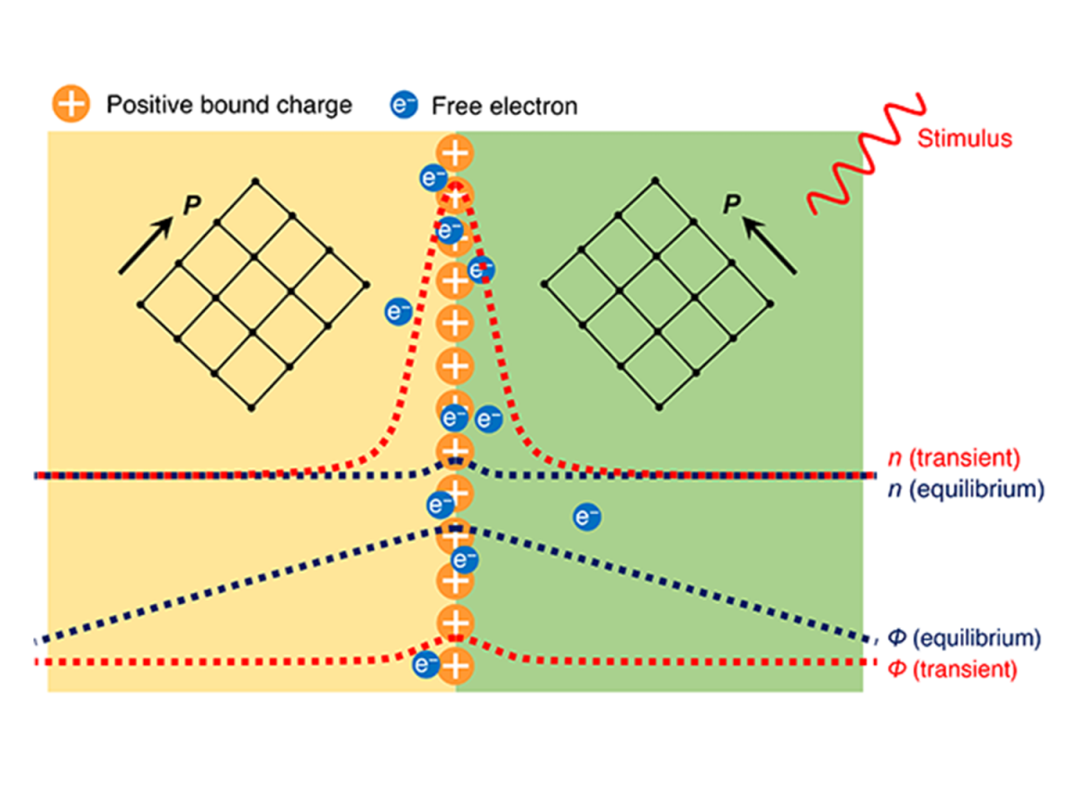
A newly developed model may serve as a bridge between quantum mechanical calculations at the atomic scale and devices that could enable next-generation quantum technologies, according to a team of Penn State researchers.
“We establish a new computational model for understanding the dynamics of simultaneous structural and electronic processes in functional and quantum materials, discovering their mesoscale fundamental physics and predicting their functionalities,” said Tiannan Yang, an assistant research professor in materials science and engineering.
The findings, published in the journal NPJ Computational Materials, represent an advance in the phase-field model—a tool for modeling how the internal structures of materials evolve at the mesoscale, which refers to the size of objects and phenomena occurring between the atomic scale and those observable by the human eye, such as crystal grains, magnetic domains, junctions, and nanoscale materials and devices, the scientists said. Predicting and controlling material behaviors at this spatial scale is critical to translating quantum phenomena into functional devices and systems.
“In terms of the phase field model, this is a really important, even transformational event,” said Long Qing Chen, Donald W. Hamer Professor of Materials Science and Engineering. “We now have a phase field model that can simultaneously describe the dynamics of structural and electronic processes. This can be applied to many different problems in functional and quantum materials.”
Understanding how the atoms and electrons inside materials will respond to external stimuli, for example heat, force, electric field, or light, is essential for predicting the material properties and ultimately harnessing the materials’ functionalities, the scientists said.
The phase field method, co-developed by Chen, has emerged over the past several decades as a powerful tool to model microstructure and physical properties at the mesoscale. But the method did not take into account the dynamical interactions between electrons and the crystal lattice, an effect that becomes particularly significant in fast processes excited by strong stimuli.
“Once you hit a material with some stimulus, it is going through a lot of processes,” said Chen, who also has appointments in mathematics and engineering science and mechanics. “And a lot of times those are simultaneous electronic and structural processes. Now, we have a way to describe these together.”
The new model allows scientists to examine the dynamics of these processes—or changes that happen over very short timescales, from picoseconds to nanoseconds—like when researchers shine short pulses of lasers onto a material to alter its electronic properties.
“A lot of properties depend on frequency,” Chen said. “When you apply a field, whether mechanical, electrical, or light at different frequencies, the material will respond differently. This model now lets us look at the frequency dependence of these responses and see how the structure has actually evolved inside the material and how that connects to the properties.”
The findings offer a theoretical framework for understanding and predicting the coupled electron and structural dynamics of excited-state materials and lay the foundation for further mesoscale models for a wide variety of functional and quantum materials, the scientists said.
Quantum materials is a broad term that refers to materials with collective properties governed by quantum behavior, such as special magnetic and electronic ordering phenomena that could lead to revolutionary, next-generation technologies, like quantum computing.
The underlying physics of the phenomena inherent to quantum materials, such as strongly interacting electrons, topologically driven spin, charge, and orbital and lattice textures, will be captured by the computational phase-field method to help researchers and engineers harness the materials’ specific properties, the scientists said.
This research stems from a $2.75 million grant awarded to a Penn State-led team to improve the phase field method. The effort is part of a larger DOE project that aims to integrate computational simulation, software development and experimental validation to accelerate the development and utilization of quantum and functional materials.


